Rubidium Chloride (RbCl) Charge-Enhanced Induced-Junction (MIS/IL) Solar Cells for Low-Temperature Silicon Photovoltaics
A practical process workflow for R&D and engineering teams to build metal–insulator–semiconductor / inversion-layer (MIS/IL) solar cells using a Rubidium Chloride (RbCl) charge-enhancement layer to raise fixed charge density and improve passivation.
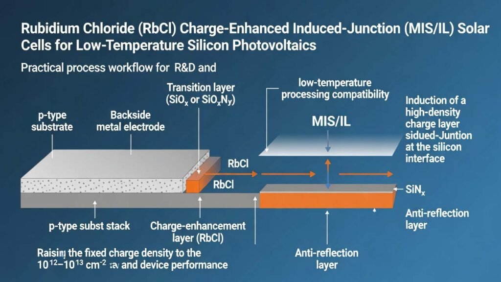
1) Overview
Induced-junction (MIS/IL) solar cells form the functional equivalent of a p–n junction by placing a thin dielectric stack with high fixed charge on a semiconductor surface. The fixed charge drives band bending and induces an inversion layer near the surface, enabling carrier separation without relying on high-temperature dopant diffusion.
This cell structure uses a p-type semiconductor substrate with a backside metal electrode and a front-side “induction layer” stack: transition layer (SiOx or SiOxNy), a charge-enhancement layer (e.g., RbCl), and an anti-reflection layer (SiNx). With an optimized charge-enhancement layer, the fixed positive charge density in the induction layer can reach the 1012–1013 cm-2 range while maintaining low interface-state density, improving surface passivation and device performance.
2) Detailed Experimental Procedure
Target device stack (front to back):
- Top electrode: Al (or Ni/Cr/Au/Ti/Pd/Ag), patterned via mask or lithography
- Anti-reflection layer (AR): SiNx (typical thickness ~70 nm via PECVD)
- Charge-enhancement layer: RbCl (single or combined with CaCl2/KCl/MgCl2)
- Transition layer: SiOx or SiOxNy
- p-type substrate: preferred p-type monocrystalline Si (0.1–10 Ω·cm, often 0.3–1 Ω·cm)
- Bottom electrode: Al (or Ti/Pd/Ag, Ti/Ag depending on deposition flow)
Recommended RbCl thickness for the charge-enhancement layer: 0.5–10 nm (commonly 1–3 nm for tight electrical/optical balance).
Process Route A: Back Electrode First + Anneal-Grown SiOx Transition Layer (Example-Oriented)
-
Substrate preparation (front side and back side):
- Start with a cleaned p-type silicon wafer (e.g., ~0.3 Ω·cm).
- Use an industry-standard silicon PV cleaning sequence to remove organics/particles/metal ions.
-
Deposit bottom electrode (back side):
- Deposit metal on the backside via thermal evaporation, sputtering, or e-beam evaporation.
- Example: thermal evaporation of Al ~5 μm on the backside.
-
First anneal (forms high-quality SiOx on the front side while protecting back metal):
- Anneal at 400–700°C for 10–120 min in H2, NH3, inert gas, or mixtures (often NH3 favored).
- Example: 550°C in NH3 for 40 min.
This anneal route is designed to avoid oxidizing the backside Al while still forming a useful front transition oxide.
-
Apply RbCl charge-enhancement layer on the front side (spin-coating option):
- Prepare a saturated RbCl solution (control insolubles; filter if needed for uniform films).
- Dispense at the front-side center and spin-coat:
- Low-speed spread: 800 rpm, 6 s
- High-speed thin-down: 2000–3000 rpm, 20–40 s (typical: 2500 rpm, 30 s)
- Soft bake: 75°C for 20 min.
-
Deposit top electrode (front side):
- Deposit metal (often Al) by sputtering/thermal evaporation/e-beam evaporation (e-beam common).
- Pattern via shadow mask or photolithography (dense grid is commonly used for lower series resistance).
-
Deposit SiNx anti-reflection layer (uncovered regions):
- Grow SiNx by PECVD (or other PVD/CVD variants) on areas not covered by the top electrode.
- Example PECVD gas set: silane + ammonia + argon; one typical flow ratio: 20:40:5
- Example process: 300°C, 20 Pa, thickness ~70 nm
-
Second anneal (final passivation enhancement):
- Anneal at 150–500°C for 5–60 min in H2, NH3, inert gas, or mixtures.
- Example: 200°C in H2 for 25 min.
Process Route B: Front Transition Layer by PECVD SiOxNy + Ultra-Thin RbCl by Evaporation
-
Substrate preparation:
- Clean p-type silicon wafer (e.g., ~0.5 Ω·cm) using standard PV-grade cleaning.
-
Deposit transition layer (front side SiOxNy):
- Use PECVD (preferred for tool compatibility), sputtering, direct oxidation/nitridation, or ion implantation approaches.
- PECVD example: SiH4 + N2O with flow ratio in 0.1–1 range (often 0.2–0.5), temperature 200–400°C (often 300–350°C), pressure 10–50 Pa (often 15–40 Pa).
- Example: SiH4:N2O = 2.5:10, 320°C, 20 Pa.
-
Deposit bottom electrode (back side):
- Form backside metal stack by e-beam evaporation, sputtering, or thermal evaporation.
- Example stack: p-Si/Ti/Pd/Ag.
-
Deposit RbCl charge-enhancement layer (front side, PVD option):
- Deposit an ultra-thin RbCl film by thermal evaporation (commonly preferred among PVD options), sputtering, or e-beam evaporation.
- Example: ~1 nm RbCl on the transition layer.
For RbCl evaporation, raw material purity and moisture control matter: low Na/K contamination and low water uptake help stabilize electrical behavior and repeatability.
-
Deposit and pattern top electrode:
- Deposit Al (or alternative metals) via e-beam evaporation and pattern via mask/lithography.
-
Deposit SiNx anti-reflection layer:
- PECVD example: silane + ammonia + argon; one typical flow ratio: 20:40:10, 320°C, 15 Pa, thickness ~70 nm.
-
Second anneal:
- Example: 220°C in H2 for 20 min.
Process control checklist (engineer-focused):
- RbCl layer thickness: keep within 0.5–10 nm (often 1–3 nm) to balance fixed charge and optical absorption/scattering.
- Moisture management: RbCl is hygroscopic; control ambient humidity during solution handling and prior to vacuum steps.
- Contamination: limit Na/K and particulates (filter solutions; verify residue/insolubles) to reduce variability in interface states.
- Anneal atmospheres: use NH3/H2/inert as specified to tune interface chemistry while protecting metal layers.
- Tool compatibility: PECVD for transition/AR layers and evaporation for electrodes are compatible with common silicon PV lines.
3) Comparison: This Production Method vs Traditional Approaches
Traditional mass-market silicon solar cells typically create the built-in field using a high-temperature dopant diffusion process (e.g., phosphorus diffusion on p-type Si). While mature, that route can introduce issues such as heavy emitter doping side effects, diffusion-induced surface defects, “dead layer” behavior that reduces spectral response, and thermal degradation of minority-carrier lifetime.
| Item | Traditional Diffused p–n Junction | RbCl-Enhanced MIS/IL Induced Junction |
|---|---|---|
| Built-in field formation | Formed by dopant diffusion to create a p–n junction | Formed by fixed-charge dielectric stack that induces inversion (junction-like behavior) |
| Thermal budget | High-temperature diffusion and related thermal cycles | Lower-temperature stack engineering + two anneals (first: 400–700°C, second: 150–500°C), avoiding diffusion-heavy steps |
| Surface damage / recombination | Diffusion can introduce defects and recombination centers near surface | Designed to reduce interface states and enhance passivation via high fixed charge + controlled anneals |
| Passivation strategy | Often relies on emitter optimization + dielectric passivation | Relies on dielectric fixed charge density (1012–1013 cm-2) and low interface-state density for strong field-effect passivation |
| Manufacturing complexity | Mature but diffusion adds high-temp equipment and process constraints | Thin-layer deposition (spin/PVD/PECVD) + anneals; compatible with PECVD and evaporation tools |
| Cost lever | Higher thermal energy and diffusion consumables | Lower-cost thin inorganic chlorides as charge enhancers + simplified junction formation pathway |
A key practical distinction is the first anneal: conventional MIS/IL routes may oxidize backside Al in dry oxygen (creating insulating Al2O3 that later requires removal), whereas the described workflow uses protective atmospheres to avoid metal oxidation while still forming a functional front transition oxide. The added second anneal is used to further reduce interface-state density and strengthen passivation.
4) Why Use Rubidium Chloride (RbCl) in This Application
In induced-junction solar cells, the induction layer’s electrical quality is the performance engine. The charge-enhancement layer is where Rubidium Chloride (RbCl) becomes strategically valuable: it is a thin, inorganic chloride that can be deposited by spin coating (from saturated solution) or physical vapor deposition (thermal evaporation/e-beam/sputter) to help the dielectric stack reach high fixed charge density while supporting low interface-state density after appropriate annealing.
Engineering advantages of RbCl as a charge-enhancement raw material:
- High fixed-charge enabling behavior: supports induction-layer fixed charge in the 1012–1013 cm-2 regime, strengthening inversion formation and carrier separation.
- Lower interface-state density pathway: with the two-anneal strategy, interface-state density can be driven down further, improving field-effect and chemical passivation synergy.
- Non-toxic alternative to cesium-based enhancers: avoids toxic cesium-compound handling while still achieving strong charge enhancement.
- Process flexibility: compatible with both solution (spin) and vacuum (PVD) methods, letting teams choose based on line capability and uniformity targets.
- Cost-down potential: inexpensive inorganic chlorides used at nanometer-scale thickness can reduce material cost contribution while enabling simpler junction formation.
- PV toolchain compatibility: integrates with standard PV equipment (PECVD, evaporation/sputter, anneal furnaces) without requiring dopant diffusion infrastructure for junction formation.
Performance indicators you can monitor to validate RbCl effectiveness:
- Fixed charge density: track C–V or related characterization; target 1012–1013 cm-2 order.
- Interface-state density (Dit): ensure charge enhancement does not come at the cost of higher Dit; the two-anneal sequence is intended to push Dit lower.
- Minority-carrier lifetime: use lifetime testing (e.g., WT-1000 class tools) as a direct proxy for passivation quality improvements.
- Optical response: verify that the AR layer and electrode layout preserve short-wavelength response benefits typical of MIS/IL designs.
For reproducibility, prioritize RbCl raw material specifications that matter in thin-film PV: low moisture, low Na/K, and low insolubles to stabilize interface chemistry and electrical dispersion. The synthesis method mentioned in this article references patent document number CN202010849725.3