Rubidium Iodide (RbI) Electron-Injection Layer Design for High-Efficiency Organic Light-Emitting Devices (OLEDs)
Audience: R&D engineers and process engineers developing low-voltage, high-efficiency OLED stacks (display and lighting), with a focus on RbI-enabled electron injection layers (EIL) co-engineered with lanthanide/alkaline-earth metals and an Ag-rich cathode.
1) Overview and Technical Value
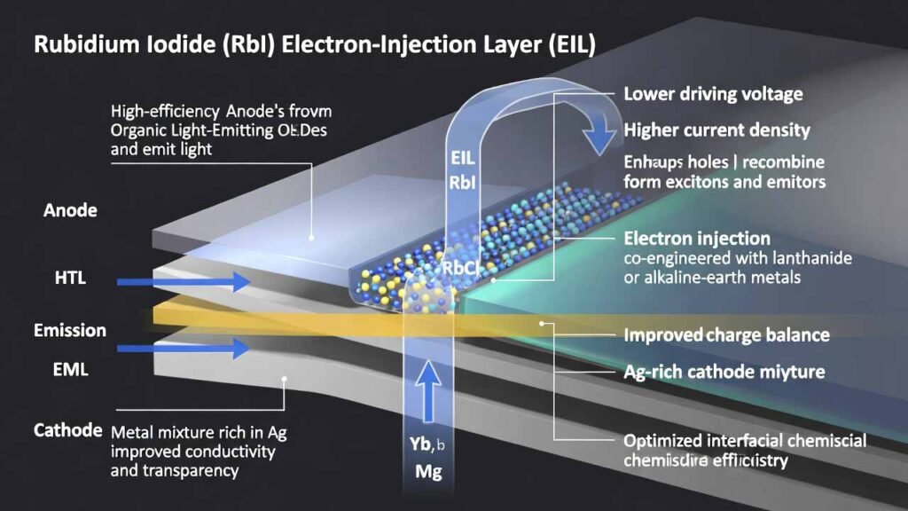
Organic light-emitting devices (OLEDs) are self-emissive stacks where holes (from the anode) and electrons (from the cathode) recombine in the emission layer (EML) to generate excitons and light. Beyond the EML, functional interlayers—hole injection/transport, electron transport, and especially the electron injection layer (EIL)—are decisive for lowering driving voltage, improving charge balance, and boosting luminous efficiency.
In this OLED architecture, the electron transport region includes an EIL formed from: (i) a Group-1 alkali halide (with RbI as a key option, optionally alongside RbCl), plus (ii) a lanthanide or alkaline-earth metal (e.g., Yb or Mg). The cathode directly contacts the EIL and is designed as an Ag-rich metal mixture (Ag as the majority component, with Mg or Yb as the secondary component).
The technical value of using RbI in the EIL is twofold:
- Lower driving voltage + higher current density at the same voltage by improving interfacial electron injection from the cathode into the organic stack.
- Improved optical transparency at the interface via interfacial chemistry between RbI and reactive metals (e.g., Yb), enabling better film appearance and potentially reduced optical loss near the cathode side.
2) Detailed Experimental Process
2.1 Device Stack Concept (Layer Order)
A representative OLED stack includes: Substrate / Anode / Hole-transport region / Emission layer / Electron-transport region / Cathode. The electron-transport region contains an EIL engineered using RbI (optionally with RbCl) plus a lanthanide/alkaline-earth metal.
2.2 EIL Design Rules (Key Ranges)
- EIL thickness: 1 Å to 50 Å (typical working window: ~10 Å to ~30 Å).
- Formation method: co-deposition of (RbI or RbCl) with a metal such as Yb or Mg, or a 2-layer EIL (alkali halide layer + metal layer, order selectable).
- Volume ratio (alkali halide : metal): 1:9 to 9:1 (common center point: 1:1).
- Cathode: Ag-rich co-deposited cathode contacting the EIL (Ag:Mg or Ag:Yb), with first metal (Ag) ≥ second metal (Mg/Yb). Typical volume ratio range: 50:50 to 99:1.
2.3 Transparency Check (Film-Level Screening)
Purpose: verify that introducing RbI changes the optical appearance of the metal interface (especially with Yb), supporting a transparent interfacial reaction layer.
- Sample A (reference): co-deposit Alq3 and Yb on a glass substrate to form a laminated film.
- Sample B (RbI-enabled): deposit Alq3/RbI (30 Å) and then deposit Yb (100 Å) on glass to form a laminated film.
- Observation: the Alq3/Yb film tends to appear opaque, while the Alq3/RbI/Yb structure appears transparent, indicating an interfacial reaction associated with RbI.
2.4 Electron-Only Device (EOD) Build for Electron Injection Evaluation
Purpose: quantify electron injection improvements by comparing current density vs. voltage (J–V) for an RbI+metal co-deposited EIL against a baseline EIL made by depositing RbI alone.
A) Substrate / Anode Preparation
- Use an ITO glass substrate (e.g., Corning ITO; ITO thickness ~1,200 Å; sheet resistance noted as 15 Ω/cm² in the source procedure).
- Ultrasonic clean for 5 minutes in isopropanol, then 5 minutes in pure water.
- UV exposure for 30 minutes and ozone cleaning (UV-ozone) to improve surface cleanliness and wettability.
B) Layer Deposition (Representative EOD Example)
Deposit sequentially by vacuum deposition (thickness in Å):
- Hole-blocking layer: Alq3, 1,000 Å.
-
Emission layer (for color-dependent EOD screening):
- Red EML: CBP (host) 98 wt% + PtOEP (dopant) 2 wt%, 300 Å.
- Green EML: same structure, replace dopant with Ir(ppy)3.
- Blue EML: AND (host) + DPAVBi (dopant).
- Electron transport layer (ETL): Alq3, 300 Å.
- Electron injection layer (EIL): co-deposit RbI and Yb at 1:1 volume ratio to a thickness of 15 Å.
- Cathode: co-deposit Ag and Mg at 5:1 volume ratio to a thickness of 90 Å.
C) Comparative Baseline (Non-co-deposited EIL)
Keep the same stack, but form the EIL by depositing RbI alone (15 Å) instead of co-depositing RbI + Yb. This isolates the effect of RbI’s interfacial synergy with the metal co-component.
2.5 Full OLED Device Build (Representative Red/Green/Blue)
Below is a representative full OLED procedure emphasizing the RbI-enabled EIL and the Ag-rich cathode.
A) Substrate / Anode Prep
Same as section 2.4A (isopropanol + water ultrasonic cleaning, UV-ozone treatment).
B) Hole-Side Layers
- Hole injection / blocking layer: 2-TNATA, 600 Å.
- Hole transport layer (HTL): NPB, 300 Å.
-
Emission layer (EML), 300 Å:
- Red: CBP 98 wt% + PtOEP 2 wt%
- Green: replace dopant with Ir(ppy)3
- Blue: AND (host) + DPAVBi (dopant)
C) Electron-Side Layers
- ETL: Alq3, 300 Å.
- EIL (key step): co-deposit RbI and Yb at 1:1 volume ratio to a thickness around 15 Å (within the general 1–50 Å EIL design window).
- Ag-rich cathode: co-deposit Ag and Mg at 5:1 volume ratio to a thickness of 90 Å (Ag is the majority component).
D) Optional EIL Architectures
- Co-deposited single EIL: RbI (or RbI+RbCl) + Yb/Mg mixed layer.
- Bilayer EIL: (RbI-based layer) + (Yb/Mg layer) with either deposition order; each layer can be 1–49 Å provided the total is 1–50 Å.
3) Comparison vs. Traditional Approaches (Process & Performance Summary)
Traditional OLED electron injection is often constrained by interfacial barriers, unstable low-work-function metals, or optical losses near the cathode side. In the provided test structures, two contrasts are especially informative:
A) Co-deposited RbI + Metal EIL vs. RbI-Only EIL
- RbI-only EIL (vacuum deposited): acts as an alkali-halide interlayer but shows weaker electron injection in the comparative J–V results.
- RbI + Yb co-deposited EIL: delivers higher current density at the same voltage across red/green/blue test devices, indicating higher electron injection efficiency.
B) Metal-Only Interface vs. RbI-Enabled Interface (Optical Behavior)
- Alq3/Yb film: tends to be opaque in the transparency screening.
- Alq3/RbI/Yb film: tends to become transparent, supporting a beneficial interfacial reaction state enabled by RbI.
From a manufacturing standpoint, the RbI-based EIL approach is also process-friendly: it stays within ultra-thin thickness windows (1–50 Å) and supports either co-deposition (single mixed layer) or bilayer stacking (process flexibility for different toolsets and stability targets). Pairing this EIL with an Ag-majority cathode (Ag:Mg or Ag:Yb) further supports low-voltage operation while reducing reliance on highly reactive metals as the dominant cathode component.
4) Why Use Rubidium Iodide (RbI): Practical Advantages in This Application
In this OLED electron-injection design, RbI is not a passive additive—it is the key Group-1 halide that enables a high-performance EIL when paired with lanthanide/alkaline-earth metals and an Ag-rich cathode. Key advantages include:
- Enhanced electron injection at the cathode interface: RbI promotes formation of ionic species and interfacial states that reduce the effective injection barrier, reflected by higher current density at the same bias when co-deposited with Yb/Mg.
- Ultra-thin effectiveness: performance benefits are achieved with only ~15 Å EIL thickness (within 1–50 Å), minimizing series resistance and optical interference.
- Transparency improvement with reactive metals: RbI can react with metals like Yb to form an optically transparent laminated interface, which is favorable for device optics and appearance.
- Compatibility with Ag-majority cathodes: using Ag as the dominant cathode component (Ag > Mg/Yb) can support better stability and manufacturability than cathodes dominated by highly reactive metals, while RbI-based EIL helps keep injection efficient.
- Process flexibility: supports either co-deposited mixed EILs (RbI + metal) or bilayer EILs (RbI layer + metal layer) with reversible order, allowing tuning for different emitters (R/G/B), ETLs, and target lifetimes.
RbI Handling & Process Notes for R&D
- Moisture control: RbI is moisture-sensitive; store and load under dry conditions to avoid interfacial contamination.
- Thickness discipline: stay in the 1–50 Å window; many teams find ~10–30 Å a practical center for optimization.
- Ratio screening: start at 1:1 (RbI:Yb) and scan within 1:9 to 9:1 to map J–V gain vs. stability and transparency.
- Cathode pairing: keep Ag as the majority metal (e.g., Ag:Mg 5:1) while using the RbI-based EIL to preserve strong injection.