CsF & RbF Electron-Selective Passivated Contacts for Crystalline Silicon Solar Cells (c-Si PV)
This page organizes a practical, engineering-oriented workflow for building electron-selective passivated contacts on crystalline silicon solar cells using cesium fluoride (CsF), rubidium fluoride (RbF), and related cesium/rubidium compounds as the key interface materials.
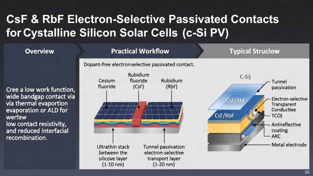
1) Overview and Technical Value
Crystalline silicon (c-Si) remains the most mature and widely deployed photovoltaic platform. The next efficiency gains increasingly depend on reducing carrier recombination and contact resistance at the c-Si/metal interface, while simplifying process complexity and lowering cost. Conventional architectures (e.g., direct metal contacts on lightly doped silicon in standard PERC) can suffer from interface defects, Fermi-level pinning, sizable Schottky barriers, and high recombination at the contact region.
A carrier-selective passivated contact addresses these losses by inserting an ultrathin stack between silicon and the electrode: a tunnel passivation layer (typically 1–10 nm) plus an electron-selective transport layer (typically 1–20 nm). In this approach, CsF and RbF (and closely related Cs/Rb halide/fluoride compounds) serve as electron-selective materials with low effective work function and large bandgap, enabling:
- Ohmic-like electron extraction with very low contact resistivity when properly engineered with the tunnel layer and metal stack
- Suppressed hole transport via a large valence-band barrier, improving selectivity and reducing recombination
- Lower parasitic optical absorption than many doped silicon layers used in traditional passivated-contact concepts
- Low-temperature processing compatibility (vacuum thermal evaporation or ALD), supporting higher throughput and simpler toolsets
- Tunnel passivation layer: saturate interfacial defects and enable tunneling transport
- CsF/RbF layer: induce downward band bending, enhance electron selectivity, lower effective work function
- Metal electrode: collect carriers with minimized interface recombination and minimized series resistance
- Tunnel passivation: 1–10 nm (SiOx, Al2O3, TiO2, ZnO, intrinsic a-Si:H, intrinsic a-SiC:H)
- Electron-selective CsF/RbF: 1–20 nm
- TCO (optional front stack): 20–200 nm (SnO2, ITO, IZO)
- ARC: 20–200 nm (SiO2, SiNx, MgF2, Al2O3 or multilayers)
- Metal: 200 nm–2 μm (Al, Mg, Ag, Au, Pd or combinations)
2) Detailed Experimental / Process Workflow
Below is a step-by-step process flow. You can implement the electron-selective passivated contact as a front-end or rear-end structure. The core differentiator is the insertion of a CsF/RbF-based electron-selective transport layer on top of a tunnel passivation layer, deposited by vacuum thermal evaporation or ALD.
A. Substrate Preparation (c-Si wafer)
- Wafer selection: choose crystalline silicon wafers per target architecture (commonly n-type for rear electron contact development). Typical thickness around 180 ± 20 μm.
- Double-side texturing: perform alkaline texturing (e.g., KOH-based) to form light-trapping surface morphology.
- Cleaning: conduct standard RCA cleaning, rinse with DI water, and dry (N2 blow and/or hot plate).
B. Front-Side Junction and Optical/Electrical Stack (example route)
- Emitter formation: create the required front-side emitter (example: boron emitter using BBr3 source for a p+ emitter on n-Si), then remove unwanted diffusion at the rear/edges as needed.
- Front surface passivation: deposit a passivation layer such as Al2O3 (e.g., ALD) with thickness in the ~10 nm class depending on optimization targets.
- Anti-reflection coating: deposit SiNx or related ARC stack (typ. ~80 nm class, adjusted for optical design).
- Front metallization: form the front electrode using screen-printed Ag paste and firing, or an alternative metallization route aligned with your process line.
- Optional front-end electron-selective stack (if implementing the passivated electron contact on the front): deposit tunnel passivation + CsF/RbF layer first, then a transparent electrode (SnO2/ITO/IZO), then ARC, then metal grid.
C. Rear Electron-Selective Passivated Contact (CsF/RbF core)
-
Deposit tunnel passivation layer (1–10 nm) on the rear c-Si surface.
- Common choices: SiOx (including LPCVD-grown ultrathin tunnel oxide), Al2O3, TiO2, ZnO, intrinsic a-Si:H, or intrinsic a-SiC:H.
- Goal: reduce interface defect density and enable carrier tunneling while maintaining strong passivation.
-
Deposit electron-selective transport layer (1–20 nm) using CsF, RbF, or a controlled mixture/stack of cesium/rubidium compounds.
- Method 1: Vacuum thermal evaporation
- Load high-purity CsF/RbF source material into a compatible crucible/boat designed for fluoride salts.
- Pump down to high vacuum (typical base pressure in the 10-4 Pa class, or as low as your tool allows).
- Evaporate at a stable low rate suitable for sub-10 nm control (engineers often run in the ~0.01–0.05 nm/s class for ultrathin layers; tune per source/geometry).
- Target thickness: start with 2–6 nm as an initial screening window, then map 1–20 nm for process window and contact optimization.
- Method 2: ALD
- Use an ALD process capable of forming uniform ultrathin fluoride layers or fluoride-containing compounds with precise thickness control.
- Target thickness: 1–20 nm with sub-nm control for contact resistivity vs. passivation trade-off mapping.
- Handling note: CsF and RbF are moisture-sensitive; minimize ambient exposure, use dry storage, and consider in-situ transfer when available.
- Method 1: Vacuum thermal evaporation
-
Deposit rear metal electrode (200 nm–2 μm).
- Use thermal evaporation or other compatible deposition to form the metal stack (e.g., Al primary contact layer plus Ag capping layer for conductivity and stability).
- Typical engineering practice: deposit an initial Al layer (order 100 nm) followed by a thicker Ag layer (order 300 nm) where appropriate, then adjust to your line’s metallization strategy.
-
Optional post-deposition anneal to stabilize contact and reduce defects.
- Run in inert atmosphere (N2) with a temperature window chosen to maintain ohmic behavior and passivation integrity.
- In similar alkali-halide contact concepts, ohmic contact can remain stable up to a moderate temperature regime; validate your CsF/RbF stack with TLM after each anneal condition.
D. Device Characterization (R&D Checklist)
- J–V under standard illumination: extract Voc, Jsc, FF, and efficiency to quantify the benefit of electron-selective passivated contact insertion.
- TLM contact resistivity (ρc): map ρc versus CsF/RbF thickness (1–10 nm screening first, then widen).
- Work function / interface energetics: use XPS/UPS (or quasi in-situ measurements) on CsF/RbF/metal stacks to confirm low effective work function and metal “insensitivity” trends.
- Thermal stability: anneal matrix (e.g., stepped temperatures in N2) and re-measure ρc and device metrics.
- Optical parasitic absorption: confirm that the ultrathin CsF/RbF layer contributes minimal absorption compared with heavily doped silicon layers.
3) Comparison vs Traditional Approaches (Summary for Engineers)
- Metal directly contacts lightly doped silicon in localized regions
- Interface recombination can be severe; contact resistance can be non-trivial
- May require additional patterning steps (e.g., laser openings) and complex optimization
- Doping and contact formation can introduce additional recombination mechanisms and optical losses
- Excellent passivation and selectivity, but often relies on doped poly-Si or doped a-Si layers
- Equipment and process can be complex; dopant gases can be hazardous and costly
- Parasitic absorption can rise due to doped layers
- Thermal stability constraints may limit some downstream steps
- Uses wide-bandgap, low-work-function CsF/RbF (and related Cs/Rb compounds) to realize electron selectivity
- Low-temperature, thin-film compatible routes (thermal evaporation / ALD)
- Reduced reliance on heavy doping steps and associated gases
- Targets low ρc and reduced interfacial recombination with a tunnel passivation assist
Practically, the CsF/RbF pathway aims to combine the contact-quality advantages of passivated contacts with a simpler, lower-temperature deposition toolkit and a thin, optically benign electron-selective layer, improving both manufacturability and performance headroom.
4) Why CsF, RbF, and Related Cesium/Rubidium Compounds Are Advantageous Here
The electron-selective layer is the “workhorse” interface that controls band alignment, carrier selectivity, and contact resistivity. Selecting CsF and RbF (or engineered stacks/mixtures with other cesium/rubidium compounds) provides several practical advantages:
CsF/RbF-based ultrathin films can create favorable band bending at the n-Si surface, helping form an electron-accumulated region that supports ohmic-like electron transport while maintaining a large barrier for holes. This directly reduces interfacial recombination and contact losses when paired with a tunnel passivation layer.
Fluoride-based layers are wide-bandgap and extremely thin (nm-scale), which supports low parasitic absorption compared with many doped transport layers, protecting Jsc and overall optical utilization of the c-Si absorber.
Alkali-compound interlayers are often less sensitive to the choice of metal electrode because the interlayer strongly influences the effective work function seen at the interface. This can broaden electrode options (Al/Ag/Mg stacks, etc.) and ease integration into existing metallization schemes.
CsF/RbF can be deposited by scalable thin-film methods (thermal evaporation or ALD) with precise thickness control in the 1–20 nm range, enabling a wide process window for R&D optimization and potential industrialization.
Raw Material Guidance (What R&D Teams Should Specify)
- Purity: specify high purity grades to minimize metal/oxide contamination that can degrade interface passivation and raise ρc.
- Moisture control: require low moisture content and moisture-barrier packaging; CsF/RbF are moisture-sensitive and should be handled in dry conditions.
- Thermal evaporation suitability: request particle size and morphology suitable for stable evaporation, minimizing spitting and thickness non-uniformity.
- Formulation options: consider CsF/RbF single layers, bilayers, or co-deposited mixtures to tune selectivity, stability, and interface energetics.
- Compatibility: verify compatibility with your tunnel passivation chemistry (SiOx, Al2O3, etc.) and downstream metallization/anneal steps.
Practical starting point for optimization: Build a thickness matrix for CsF and RbF (e.g., 1, 2, 3, 4, 5, 10 nm) on your chosen tunnel layer, measure ρc via TLM and correlate with device J–V. Then expand to mixed CsF/RbF stacks if you need a wider stability/process window.
Done well, the CsF/RbF electron-selective contact approach can reduce contact recombination and contact resistance simultaneously, while keeping the process low-temperature, thin-film-friendly, and scalable.