Rubidium Sulfate–Enabled High-Efficiency OLEDs for Displays and Solid-State Lighting
Overview
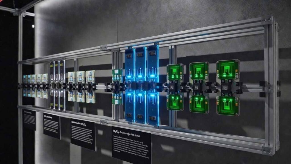
This OLED device architecture is built as a multilayer stack designed to increase electron injection efficiency and improve charge balance in the emissive zone. The device includes, in sequence, an anode, hole injection layer (HIL), hole transport layer (HTL), emissive layer (EML), electron transport layer (ETL), an electron injection layer (EIL), and a cathode. The key functional upgrade is the EIL: it is formed from a rubidium compound combined with a magnesium compound. For engineering implementation, rubidium sulfate (Rb2SO4) is a practical rubidium-source option for the EIL because it participates directly in forming the injection structure that boosts electron transport, supports n-type interaction with ETL materials, and contributes to higher luminous efficiency.
Detailed Manufacturing Process
-
Anode preparation (conductive glass selection and patterning)
- Select anode substrate: ITO (preferred), FTO, AZO, or IZO; typical anode thickness range 50–300 nm (example value: ~80 nm).
- Photolithography and dicing to the required size.
- Ultrasonic cleaning sequence (each ~15 min): detergent → deionized water → acetone → ethanol → isopropanol to remove organics and residues.
- Optional surface activation: oxygen plasma treatment (~5 min, ~30 W) to improve interface quality and wettability for subsequent layers.
-
Vacuum system and base process control
- Use a high-vacuum coating system for organic and inorganic deposition.
- Maintain clean tooling to minimize contamination, especially for the ultrathin EIL (1–8 nm) where defects directly impact injection.
-
Form HIL, HTL, EML, and ETL (vacuum deposition sequence)
- Deposit functional layers on the anode surface in order: HIL → HTL → EML → ETL.
-
Example material options:
- HIL: MoO3, WO3, V2O5 (example: MoO3).
- HTL: TAPC, TCTA, NPB (example: NPB).
- EML: DCJTB, ADN, BCzVBi, Alq3 (example: Alq3).
- ETL: Bphen, TAZ (triazole derivatives), TPBI (example: Bphen).
- Typical vacuum evaporation window for organic layers: vacuum pressure around 5×10⁻³ to 2×10⁻⁴ Pa; deposition rate about 0.1–1 nm/s (application-specific optimization recommended).
- Thickness design is application-dependent (examples from representative stacks): HIL ~20–80 nm; HTL ~20–60 nm; EML ~0.5–40 nm; ETL ~40–250 nm.
-
Build the Electron Injection Layer (EIL) using Rubidium Sulfate as the rubidium raw material
- Prepare EIL source materials: Rb2SO4 (rubidium sulfate) + one Mg compound (e.g., MgCl2 / MgF2 / MgO / MgS).
- Set the EIL mass ratio: Rb2SO4 : Mg compound = 5:1 to 8:1 (example configuration: 7:1).
- Deposit the EIL by electron-beam evaporation (or resistive evaporation where applicable) onto the ETL surface. Recommended control target: EIL thickness 1–8 nm (example: 5 nm).
- Example electron-beam evaporation process window: working pressure 2×10⁻³ to 5×10⁻⁵ Pa, energy density 10–100 W/cm2, organic deposition rate 0.1–1 nm/s, metal/metal-compound deposition rate 1–10 nm/s.
- Engineering note for Rb2SO4 handling: keep the powder dry and minimize exposure time before loading to reduce moisture pickup; stable, repeatable evaporation and ultrathin film continuity depend on controlled raw-material condition.
-
Deposit the cathode
- Form the cathode (Ag / Al / Pt / Au; example: Ag or Al) on top of the EIL.
- Deposition method: magnetron sputtering or vacuum deposition consistent with the selected cathode metal. Typical cathode thickness range: 80–250 nm (example: ~150 nm).
-
Representative device example using rubidium sulfate
- Example stack: ITO / V2O5 / NPB / BCzVBi / TPBi / (Rb2SO4:MgCl2) / Al
- Example EIL setting: Rb2SO4:MgCl2 = 7:1, thickness 5 nm.
- Example electron-beam evaporation setting: pressure 2×10⁻⁴ Pa, energy density 50 W/cm2, organic rate 0.5 nm/s, metal/compound rate 6 nm/s.
-
Electrical/optical characterization (for process feedback)
- Measure EL spectrum, current density–efficiency behavior, and stability under controlled current density.
- Use results to tune EIL thickness (1–8 nm) and Rb2SO4:Mg ratio (5:1–8:1) for optimal injection/charge balance.
Comparison vs. Traditional OLED Electron Injection Approaches
Traditional OLEDs commonly use LiF as the electron injection layer. In practice, LiF-based EILs can be challenging in vacuum manufacturing because deposition can require harsher conditions, which raises the risk of thermal or process-induced damage to adjacent organic functional layers. In addition, LiF films may show weaker film-forming behavior at ultrathin thickness, increasing the likelihood of injection defects and exciton quenching pathways, which reduces the probability of electron–hole recombination in the emissive layer.
In contrast, the Rb-compound + Mg-compound EIL approach introduces a tunable composite injection structure. The rubidium compound component (here, Rb2SO4 as the rubidium raw material) supports improved electron transport behavior through interaction with the ETL and enables a higher recombination probability, while the Mg compound component (with relatively larger particle size behavior in the composite concept) promotes light scattering, helping more photons exit through the substrate side and improving external emission.
Why Rubidium Sulfate and This Process Improve OLED Applications
- Direct function in the critical EIL: Rubidium sulfate is not a minor additive; it is a primary rubidium-source raw material used to build the electron injection layer that governs carrier injection at the ETL/EIL/cathode interface.
- Higher electron transport and better charge balance: The rubidium-based EIL can enhance electron transport and increase electron–hole recombination probability in the emissive layer, translating into higher luminous efficiency for display and lighting stacks.
- Process tunability for engineering optimization: The EIL is adjustable through two knobs that are simple to control in production: mass ratio (5:1–8:1) and thickness (1–8 nm), enabling fast DOE loops for different emitters and ETL materials.
- Optical extraction support via Mg compound pairing: Pairing Rb2SO4 with a magnesium compound (e.g., MgCl2) can increase light scattering within the stack and encourage substrate-side outcoupling, supporting higher perceived brightness at the same drive current.
- More robust device efficiency behavior under varying current density: Devices built with the rubidium-compound/Mg-compound EIL structure can show improved current efficiency compared with conventional EIL baselines, indicating reduced injection loss mechanisms and better operational efficiency.
- Practical sourcing note for R&D and pilot lines: specifying Rb2SO4 purity, moisture control, and consistent powder handling helps stabilize evaporation repeatability and ultrathin film continuity, which are often the hidden yield limiters for 1–8 nm injection layers. The mentioned synthesis method references patent document number CN201310581191.0