Rubidium Iodide (RbI) Additive Engineering for MA-Free Wide-Bandgap Perovskite Tandem Solar Cells
1) Overview and Application Background
Wide-bandgap (around 1.7 eV) metal-halide perovskites are a key absorber for tandem photovoltaics (for example, perovskite/silicon stacks) because their tunable bandgap enables higher overall conversion efficiency than single-junction devices. A practical bottleneck is manufacturing: many high-performance wide-bandgap films are made by one-step spin coating, which is difficult to scale to large areas with consistent film quality.
Wide-bandgap mixed-halide perovskites also face intrinsic film-formation challenges. High bromide content can accelerate crystallization, producing small grains and high grain-boundary defect density. Under illumination, iodine–bromine mixed compositions can undergo halide phase segregation, creating iodide-rich low-bandgap domains that reduce voltage and accelerate degradation. In addition, deep-level defects at surfaces/interfaces and a high bulk trap density increase non-radiative recombination and carrier losses.
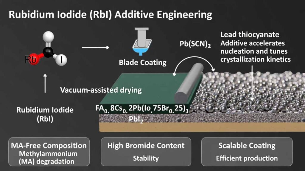
The approach here uses a methylammonium (MA)-free wide-bandgap composition FA0.8Cs0.2Pb(I0.75Br0.25)3 (bandgap ≈ 1.7 eV) to avoid MA-related degradation risk, and applies an additive pair: Pb(SCN)2 plus a rubidium salt (preferably rubidium iodide, RbI). Pb(SCN)2 accelerates nucleation and tunes crystallization kinetics, while the rubidium salt works synergistically to improve grain coalescence, suppress bulk PbI2 residue, and support dense, pinhole-free films suitable for scalable coating.
2) Detailed Experimental Procedure
2.1 Precursor Solution Formulation (MA-Free Wide-Bandgap Perovskite)
Target perovskite system: FA0.8Cs0.2Pb(I0.75Br0.25)3
Solvent: N,N-dimethylformamide (DMF)
Additives (molar basis vs. mixed solution): Pb(SCN)2 at 1–3%; rubidium salt at 2–6%. Practical example uses 1.5% Pb(SCN)2 and 3% RbI.
- Prepare a mixed precursor containing FAI, CsI, PbI2, PbBr2 in DMF. The total precursor concentration is typically 1.0–1.5 mol/L (example: 1.5 M).
- Add Pb(SCN)2 and RbI (or RbCl as an alternative rubidium salt) into the same solution.
- Mix/vibrate for ~20 minutes until fully dissolved to obtain a uniform wide-bandgap perovskite precursor solution.
Example mass-based recipe (1.5 M, 1 mL DMF): PbI2 0.432 g; PbBr2 0.206 g; FAI 0.206 g; CsI 0.078 g; 2-imidazolidinone 0.038 g; plus Pb(SCN)2 0.007 g and RbI 0.009 g. Mix/vibrate ~20 min to dissolve completely.
2.2 Substrate Preparation
- Use a conductive substrate such as ITO glass or FTO glass (example size: 2.5 cm × 2.5 cm).
- Sequentially clean with glass cleaner, ultrapure water, and absolute ethanol.
- Dry with nitrogen.
- Perform UV-ozone treatment for 15 minutes prior to layer deposition.
2.3 Charge-Transport / Interfacial Layers (Representative Device Stack)
Below is a representative sequence used in a complete device; film-only fabrication can start directly from the coating step.
- Hole-transport layer (HTL) solution: dilute 4PADBC in ethanol to 0.5 mg/mL, shake/vibrate 20 min. Spin coat 80 μL at 5000 rpm for 30 s, then anneal at 100°C for 10 min.
- Al2O3 layer: mix Al2O3 stock with isopropanol at 1:50 (v/v), shake/vibrate 20 min. Spin coat 80 μL at 5000 rpm for 30 s, then anneal at 100°C for 10 min.
- PEAI interlayer (DMF): dissolve PEAI in DMF to 1 mg/mL, shake/vibrate 20 min. Spin coat 80 μL at 5000 rpm for 30 s, then anneal at 100°C for 5 min.
2.4 Blade Coating + Vacuum-Assisted Drying + Annealing (Core Film-Formation Process)
- Dispense ~20 μL of the perovskite precursor solution into the gap between the blade and the substrate surface.
- Blade-coat at a constant speed of 5 mm/s to spread the solution uniformly.
- Immediately transfer the coated substrate into a vacuum chamber. Pump down to 10 Pa and maintain for 10 seconds to quickly extract solvent and stabilize early-stage crystallization.
- Anneal to form the perovskite film. A general window is 80–150°C for 30–60 seconds. In the representative device example, anneal at 120°C for 20 minutes to complete film formation.
The additive pair Pb(SCN)2 + RbI is used specifically to control the nucleation–growth balance under this fast, scalable coating workflow, enabling dense films with large grains and reduced defect density.
2.5 Post-Treatments and Device Completion (Representative)
- PEAI surface treatment (IPA): dissolve PEAI in isopropanol to 1 mg/mL, shake/vibrate 20 min. Spin coat 80 μL at 5000 rpm for 30 s, then anneal at 100°C for 10 min.
- Electron transport layer (ETL): vacuum-evaporate 30 nm C60.
- Buffer/oxide layer: deposit 20 nm SnO2 by atomic layer deposition (ALD).
- Back electrode: vacuum-evaporate 100 nm Ag to complete the device.
2.6 Characterization and Performance Verification
- SEM for surface morphology and grain/void inspection.
- XRD for crystal structure and phase purity; check for undesired PbI2 signatures.
- J–V measurements for photovoltaic parameters (Voc, FF, PCE) on devices (example active area: 0.093 cm²).
- MPP tracking under continuous illumination to assess operational stability (example: ~45°C).
3) Comparison vs. Conventional Approaches
| Dimension | Conventional Wide-Bandgap Perovskite Practice | Blade Coating + Vacuum with Pb(SCN)₂ + RbI |
|---|---|---|
| Scalability | One-step spin coating is common but difficult to extend to large areas with uniformity. | Blade coating is inherently scalable and can align with industrial slot-die coating workflows. |
| Crystallization Control | High-Br wide-bandgap films can crystallize too fast, leading to small grains and more grain-boundary defects. | Pb(SCN)₂ accelerates nucleation while RbI supports controlled growth and grain coalescence under fast solvent removal. |
| Residual PbI2 / Film Defects | Bulk PbI2 residue and voids/pinholes can appear, increasing recombination and instability risks. | Synergistic additives suppress bulk PbI2 residue and help form dense, pinhole-free films with larger grains (>500 nm reported). |
| MA-Related Degradation | MA-containing formulations carry a known stability risk in operational environments. | MA-free FA/Cs formulation removes MA+ degradation risk while maintaining a ~1.7 eV bandgap for tandem matching. |
| Device Metrics & Stability | Additive-free or single-additive films show limited improvement; faster decay under MPP tracking is common. | Compared with additive-free controls, Voc/FF/PCE improve noticeably; MPP tracking retained ~80% initial PCE after 320 h at ~45°C (control reached 80% in ~30 h). |
4) Why Rubidium Iodide (RbI) Matters in This Application
In this MA-free wide-bandgap mixed-halide system, RbI is not a minor additive—it is a functional raw material that helps make scalable coating viable while protecting optoelectronic quality. When combined with Pb(SCN)2, RbI supports a crystallization pathway that produces a dense film with larger, better-fused grains and fewer electronically active defects.
Key Technical Advantages Delivered by RbI (as the Rubidium Salt Additive)
- Synergy with Pb(SCN)2 for crystallization engineering: Pb(SCN)2 accelerates nucleus formation and tunes crystallization kinetics, while RbI complements this by promoting grain fusion and improving film compactness.
- Reduced bulk PbI2 residue: Films formed with Pb(SCN)2 + RbI show suppression of bulk PbI2 remnants, lowering recombination pathways and improving device consistency.
- Improved morphology for carrier transport: Dense, pinhole-free layers and larger grains support better carrier transport and reduce non-radiative recombination at grain boundaries.
- Operational stability benefit under illumination: With Pb(SCN)2 + RbI, devices maintained ~80% of initial PCE after 320 hours of MPP tracking at ~45°C, indicating substantially improved working stability versus additive-free references.
- Process compatibility with scale-up: RbI-enabled morphology control under blade coating + vacuum-assisted drying provides a practical bridge from lab coating to scalable manufacturing methods such as slot-die coating.
Engineer’s takeaway: If your goal is a scalable, MA-free ~1.7 eV wide-bandgap perovskite top cell for tandems, prioritize RbI as the rubidium salt additive and co-design it with Pb(SCN)2 under a fast solvent-removal workflow (vacuum to ~10 Pa for ~10 s), then confirm improvements via SEM/XRD and MPP stability testing.
The mentioned synthesis method references patent document number CN202510491325.2